
Fully printed
Perovskite absorbs the complete visible spectrum, so one cell performs under warehouse LEDs and under the sun. We print every functional layer, which keeps cost low and shape free.
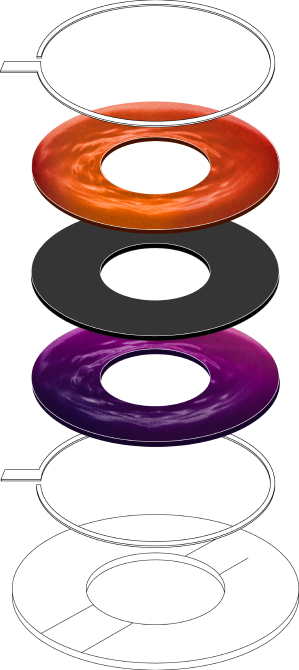
Five layers, one print run
Our architecture is printed layer by layer on the substrate, and we avoid critical raw materials.
- EncapsulationSeals the stack for a lifespan of more than 10 years.
- Back contactPrinted rear electrode that collects the current.
- PerovskiteThe absorber that turns indoor and outdoor light into current.
- Transport layersMove charges out of the absorber with minimal loss.
- SubstrateThe base the stack is printed on, cut to the shape of your device.
Layer naming simplified for this concept; to be confirmed with the Perovskia team.
Perovskite, up close
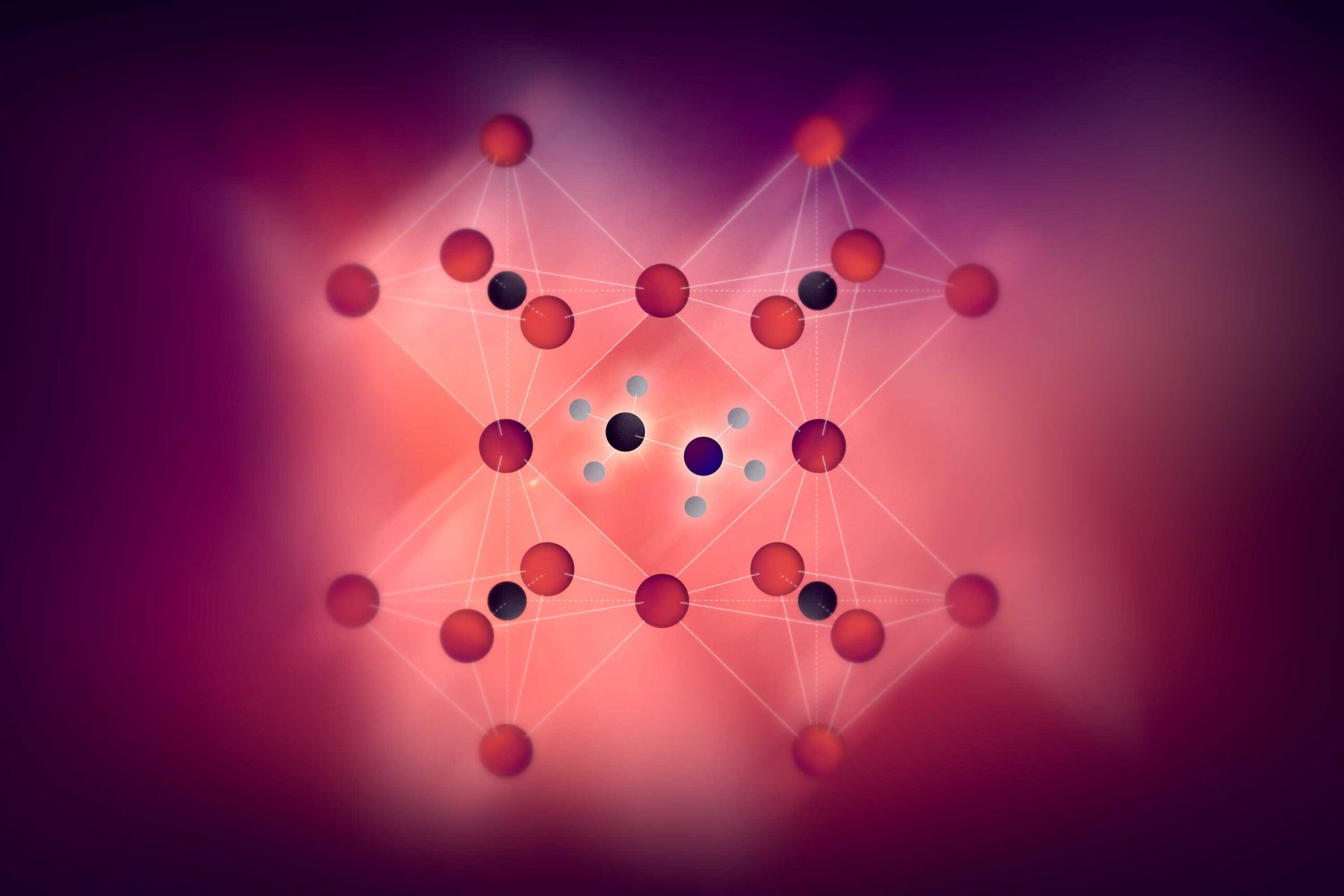
The crystal structure that gives the material its name is also why it handles low light so well. Constant R&D keeps pushing both efficiency and lifespan.
Less battery waste
Our mission is to minimise battery waste by harnessing the light that is already in the room.
Lower carbon footprint
Abundant raw materials and a much lower footprint than traditional silicon solar cells.
Recyclable by design
The product has the potential to be fully recycled, supporting a circular economy.